MOSFET Gate Driver Design: Gate Resistor, Dead Time and Bootstrap Sizing
Quick answer: a reliable MOSFET gate driver must charge and discharge the gate quickly enough to limit switching loss, but not so aggressively that ringing, EMI and false turn-on become unacceptable. Start with gate charge and switching time, select the driver peak current, then tune separate turn-on and turn-off resistance on the bench.
Start with gate charge, not input capacitance
The data-sheet gate charge curve is more useful than the headline input capacitance because it shows the charge needed through the Miller plateau. A first estimate is Igate = Qg / tsw. If total gate charge is 60 nC and the target transition is 100 ns, the average gate current during the transition is roughly 0.6 A. Choose a driver with margin because peak current, temperature and source impedance vary.
Gate resistor calculation
The initial total resistance is approximately (Vdrive − Vplateau) / Igate. Subtract the driver output resistance and the MOSFET internal gate resistance to estimate the external resistor. The calculation is only a starting point: probe drain voltage, gate voltage and current with short ground connections, then increase resistance if ringing or overshoot is excessive. A diode plus two resistors allows slower turn-on and faster turn-off.
Dead time without excess diode loss
In a half bridge, dead time prevents shoot-through when one device has not fully turned off. Too little dead time produces destructive cross-conduction; too much forces current through a body diode and raises loss. Verify dead time at the MOSFET pins under maximum temperature, current and supply voltage. Do not rely only on the controller’s programmed value.
Bootstrap capacitor sizing
The bootstrap capacitor supplies the high-side driver while its switch node is elevated. Sum MOSFET gate charge, driver quiescent charge, leakage and a safety allowance, then divide by the permitted voltage droop: Cboot ≥ Qtotal / ΔV. A 100 nC requirement with 0.2 V permitted droop needs at least 0.5 µF; select a larger low-ESR ceramic value after accounting for DC-bias derating.
Layout checklist
- Place the driver beside the MOSFET.
- Use a dedicated Kelvin source return where available.
- Keep the gate loop and bootstrap loop compact.
- Separate power and control grounds carefully.
- Add a gate-source resistor and consider a Miller clamp for fast half bridges.
FAQ
Can a very small gate resistor damage the MOSFET? Yes. It can increase voltage overshoot, EMI and false turn-on even when switching loss falls.
Should the gate be driven above its threshold voltage? Yes. Threshold is measured at tiny drain current; use the specified enhancement voltage and never exceed the absolute gate limit.
Continue with our electronics guides and electrical engineering library.
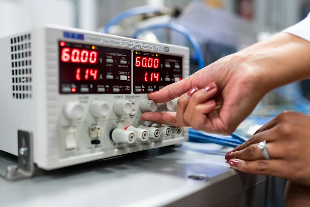
Featured photo: ThisisEngineering via Unsplash.